
SUNY Polytechnic, Silicon Carbide (SiC) pilot line
DPS have been engaged to carry out the basis of design, the detailed MEP design scope and federated model management with our client.
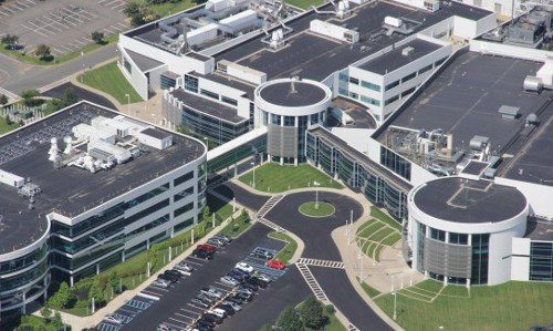
About this project
DPS have been engaged to carry out the Basis of Design, the detailed MEP design scope and federated model management with our client. The retrofit is an operational facility with multiple tenants requiring detailed shutdown scope, scheduling, planning and execution through collaboration with contractors. The team intends to ramp with the existing tool set between 6 months to 1 year, to a 5,000 wafer out/per annum capacity.
Limited as-built information required systems to be field verified in order to produce a quality, accurate design. Laser scan data was used extensively within the design model to ensure accurate detailing and co-ordination with all trades. A comprehensive analysis of the project utility requirements against the existing facility data was used to determine the utility scope required, with minimal impact to the existing operational facility. Extensive planning was performed in close cooperation with the client to ensure zero unplanned downtime due to utility interruptions.
Process/support systems
- Bulk chemicals and distribution
- Spec gases
- Bulk gases
- Waste water treatment
- Process mechanical
- HVAC
- Electrical and I&C
Facility features
The project scope requires ~8,500 SQ.FT. of process tool renovation within an existing 35,000 SQ.FT. cleanroom space, in the Nano Fab North (NFN).
- 35,000 sq. ft. ’Clean Space’
- Live facility
- Silicon Carbide manufacturing capability
- HPM expansion
- Multiple tenants in manufacturing space
Tell us about your project
and discover how DPS can help you today